LM3445EVM-695 LM3445 120Vac Valley Fill Buck Triac Dimmable LED Driver Evaluation Module. Full capabilities for printed circuit board manufacturing may extend beyond the rules below but often times involve additional processes and costs to achieve the desired results.
Passive Pfc
The advantage of using a current fed resonant inverter in the proposed power circuit is that it.
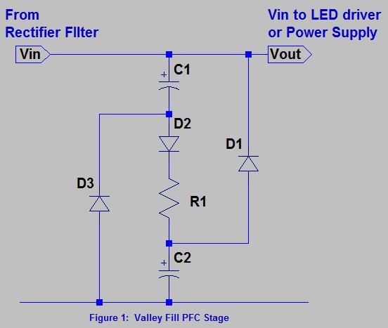
. The approach is based on the concept of negative input resistance that a SMPS presents to the filter when operated in a feedback configuration. Valley fill with passive PFC circuits B and active PFC shown C. This ballast design achieves high power factor 09 low THD.
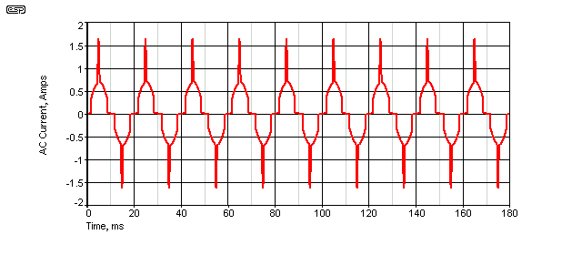
Design LM3445 SNVS570MJANUARY 2009REVISED NOVEMBER 2015. To minimize the risks. Current waveform of the passive PFC valley fill circuit.
The following parameters need to be defined and determined. IF vallyfill is possible can we use same transformer Design. IC is configured to drive a 35 W flyback power supply with a switched valley fill PFC providing a high power factor 12 V constant voltage supply throughout the input range of 140 VAC to 320 VAC.
The DC output of. Section 3022 Townhouses Added additional criteria to Section R30222 Common walls item 1. Its simple to implement but is only suitable where a very high effective ripple voltage on the DC output can be tolerated.
A switched valley-fill PFC circuit is added to meet the high PF requirement in lighting applications. This article discusses a practical approach to designing an input filter to the switch-mode power supply SMPS. Valley Select2 Control Panel Advanced Features Manual.
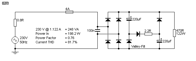
An important design parameter to consider here is deciding on the minimum switching frequency. 41 Input EMI Filter and Rectifier The input fuse F1 provides safety protection from component failures. The solution under study is based on a DC to AC resonant inverter whose input voltage is taken from a valley-fill AC-DC passive converter.
Derive raw dc voltage from the utility a line figure above. For low power applications theres a rectifier circuit known as a valley-fill rectifier. Valley Select2 Control Panel Owners Manual.
Define and determine system requirements. A diagram that represents the elements of a system using abstract graphic drawings or realistic pictures. Valley voltage 096 1 104 VRAMP V Peak voltage 285 3 308 DRAMP Maximum.
Ics and develops the fundamental circuit equations that are used throughout the book. Choose from a network of design firms to prototype and manufacture your custom PCB. PSpice for TI is a design and simulation environment that helps evaluate functionality of analog circuits.
Electrician Circuit Drawings and Wiring Diagrams Youth Explore Trades Skills 3 Pictorial diagram. 11 The common wall can contain plumbing and mechanical. Upload your Gerber file and receive a quote.
Similar equations have been developed in other books but the. Variable Rate Irrigation Prescription Software User Guide. 1 TRIAC Dim Decoder Circuit for LED Dimming buck step-down constant current controller designed Application Voltage Range 80 VAC to 277 VAC to be compatible with TRIAC dimmers.
The ballast circuit is the combination of a valley fill circuit and a new frequency modulated current fed resonant inverter. The goal of this design is to implement a low-cost linear ballast with good PFC acceptable THD and low current-crest factor. The proposed charger is based on a diode-clamped series resonant converter equipped with a resonant valley-fill circuit which increases the power factor by removing dead zones in the line current and reduces the switching loss of the valley-fill circuit.
Valley-Fill PFC Circuit. The following standard and advanced capabilities will assist printed circuit board PCB designers in setting up their basic design checks. Up to 96 cash back Design Space for Windows Set up a new Cricut product browse projects start designing and more.
TI assumes no liability for applications assistance or customer product design. A new Circuit for Low-Cost Electronic Ballast Passive Valley Fill with additional Control Circuits for Low Total Harmonic Distortion and Low Crest Factor by Cecilia Contenti Peter Green Tom Ribarich Abstract. Chapter 3 Building Planning - Climatic and Geographic Design Criteria Table R30121 3.
A diagram that uses lines to represent the wires and symbols to represent components. Customers are responsible for their products and applications using TI components. The benefit to designers is that the same control circuit topology can be applied to different applications over a wide power range thereby simplifying the design process and keeping component count low.
This simplified circuit topology now makes CCM operation practical over a broader range of power even down to below 100 W. Can we add the Valley fill circuit with this schematics to improve the PFC. The feasibility of the proposed charger has been verified with a 17-kW prototype.
The energy stored across the PFC inductor is delivered to the load via direct energy transfer reducing the power loss. Table 30121 Manual J Design Criteria Deleted Manual J Design Criteria from Table and footnote n. DER-637 using a LYTSwitch-6 IC offers an accurate fast transient response constant voltage supply with a high power factor.
While the circuitry appears very simple the design of an effective correction system is actually. This full-featured design and simulation suite uses an analog analysis engine from Cadence. Every SMPS design starts in determining the required system requirements and specifications.
Available at no cost PSpice for TI includes. Hi We have assembled and tested the DER215 12V 700mA using LNK606PGWhich was working fine as mentioned on DER215 but the Powerfactor we are getting 056we needs to improve the PFC to 089 1. The figure D are this novel PFC and regulation methodology.
Ad Quick turn custom PCBs available at Digi-Key. In this paper a novel variable frequency controller is proposed for a passive high power factor electronic ballast with dimming capability and low crest factor. April 30 2018.
Analytical discussion is followed by simulation and measurement results. This application note describes a CFL ballast using valley fill passive PFC circuit and IR2520D ballast control IC. 3 -50 Valley Fill Passive PFC Circuit Although the circuit presents a reasonably good Power Factor 095 and the harmonics can be tamed by the L-C input filter the major shortcoming of this circuit is the 50 bus ripple voltage which in a typical ballast circuit results in a crest factor exceeding 21.
Valley Fill Passive Power Factor Correction Method Power Electronics Talks

Presentation Outline Introduction To Pfc Discuss Passive Pfc Method Discuss Active Pfc Method Conclusion Ppt Download
![]()
Valley Fill Passive Power Factor Correction Method Power Electronics Talks

Pdf An Improved Valley Fill Passive Power Factor Correction Circuit For Electronic Ballast

Harmonic Content An Overview Sciencedirect Topics
Passive Pfc
Rectifier Serial Capacitors In Electronic Ballast Of A Fluorescent Lamp Electrical Engineering Stack Exchange

Pdf An Improved Valley Fill Passive Power Factor Correction Circuit For Electronic Ballast
0 comments
Post a Comment